What it is
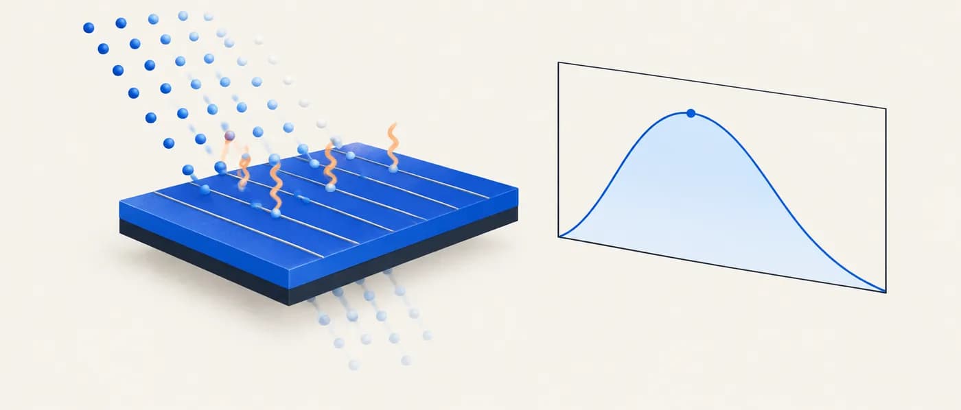
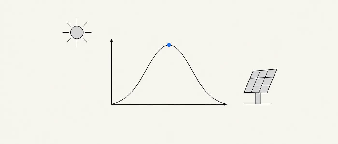
In 1961, William Shockley and Hans-Joachim Queisser calculated the maximum efficiency of a single p–n junction solar cell using detailed balance: in an ideal cell, the only unavoidable recombination is radiative, the reverse of absorption. Their limit accounts for three fundamental losses: photons below the band gap are not absorbed, photons above the gap lose their excess energy as heat, and the cell must emit some light because it is at a finite temperature.
These losses pull in opposite directions. A small gap absorbs most of the spectrum but delivers low voltage; a large gap delivers high voltage but wastes most photons. Balancing them under the standard AM1.5G spectrum gives a maximum of about 33.7% at a band gap of about 1.34 eV (the original paper, using a 6000 K blackbody spectrum, reported about 30% at 1.1 eV).
The limit applies to one absorber with one gap under one sun. Tandem and multi-junction cells, concentration, and multiple-exciton or hot-carrier concepts can exceed it, which is why it is also the benchmark those approaches are measured against.
Why it matters for R&D decisions
Band gap is the first property that decides whether a material can ever make a good solar absorber. The Shockley–Queisser curve turns a gap into an efficiency ceiling in seconds, so teams can discard materials whose ceiling is uncompetitive before measuring absorption, carrier lifetimes or defect tolerance. It also tells tandem designers which top-cell gap pairs best with a given bottom cell.
The formula
λ_cutoff (nm) ≈ 1240 / E_g (eV) · η_max(E_g) from detailed balance under AM1.5G · η_max ≈ 33.7% at E_g ≈ 1.34 eV
- E_g
- Band gap of the absorber (eV). Use the optical or fundamental gap, as appropriate
- λ_cutoff
- Longest wavelength the absorber can use; photons beyond it pass through
- η_max
- Detailed-balance maximum power-conversion efficiency for a single junction at 25 °C, one sun
- AM1.5G
- Standard terrestrial solar spectrum used for rating cells (1000 W/m²)
η_max(E_g) has no simple closed form. Use a tabulated curve such as Rühle (2016) rather than estimating it by hand.
How to apply it, step by step
- 1Get an accurate band gap
Use measured gaps where available. For computed gaps, prefer hybrid functionals (HSE), meta-GGA approaches such as TBmBJ, or GW over standard PBE, which systematically underestimates gaps.
- 2Check direct vs indirect
An indirect gap such as silicon’s absorbs weakly near the edge and needs a thicker absorber. That raises cost and demands longer carrier diffusion lengths. Note the gap type next to its value.
- 3Read the ceiling from the SQ curve
Look up η_max at your gap on a tabulated SQ curve. Treat 1.1–1.6 eV as the prime single-junction window; outside it, the ceiling falls quickly.
- 4Look beyond the gap
Gap only sets the ceiling. Absorption strength, defect tolerance, carrier lifetime and mobility decide how close a real cell gets. The Spectroscopic Limited Maximum Efficiency (SLME) adds absorption-spectrum and non-radiative-loss information.
- 5Consider tandem pairing
If the material’s gap is above the single-junction window (~1.6–1.9 eV), evaluate it as a top cell over silicon or another low-gap bottom cell rather than discarding it.
Worked examples
Reading absorption cut-offs for common absorbers
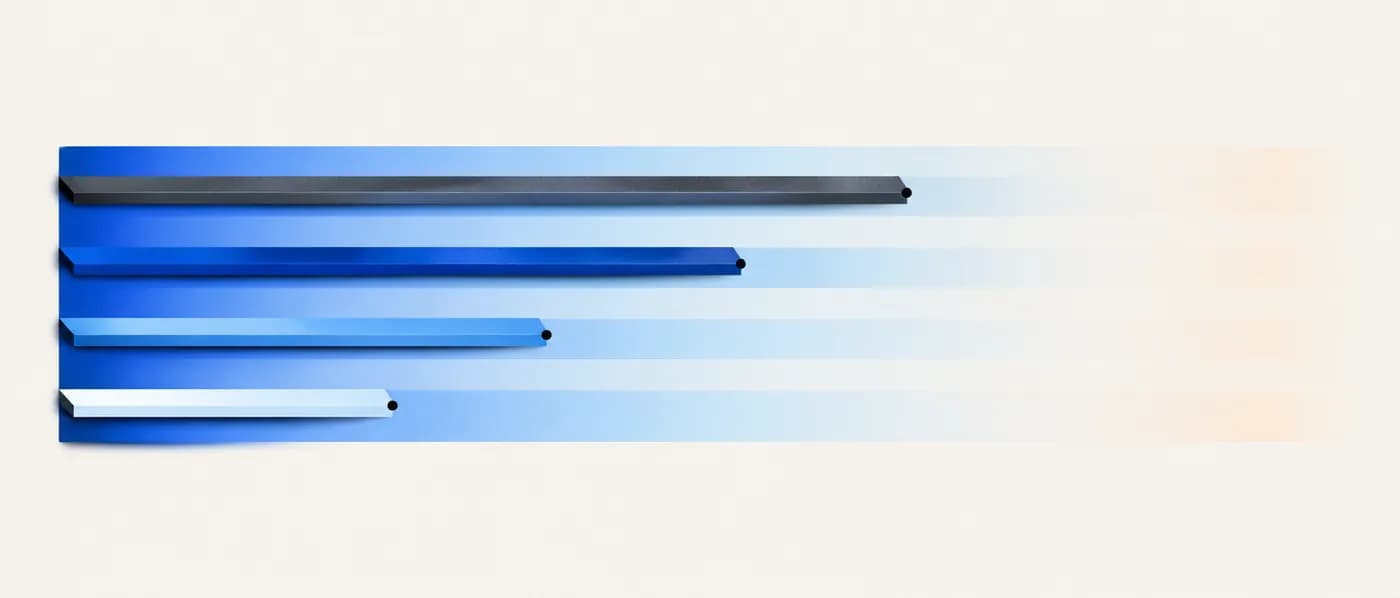
Convert band gaps into the longest usable wavelength to see how much of the spectrum each absorber can harvest.
- 01Silicon, 1.12 eV: λ ≈ 1240 / 1.12 ≈ 1,107 nm (near-infrared).
- 02The SQ optimum, 1.34 eV: λ ≈ 1240 / 1.34 ≈ 925 nm.
- 03GaAs, 1.42 eV: λ ≈ 1240 / 1.42 ≈ 873 nm.
- 04A methylammonium lead iodide perovskite, ≈ 1.6 eV: λ ≈ 1240 / 1.6 ≈ 775 nm.
All four sit in or near the 1.1–1.6 eV window, which is why they dominate single-junction research.
Rescuing a candidate from a PBE gap
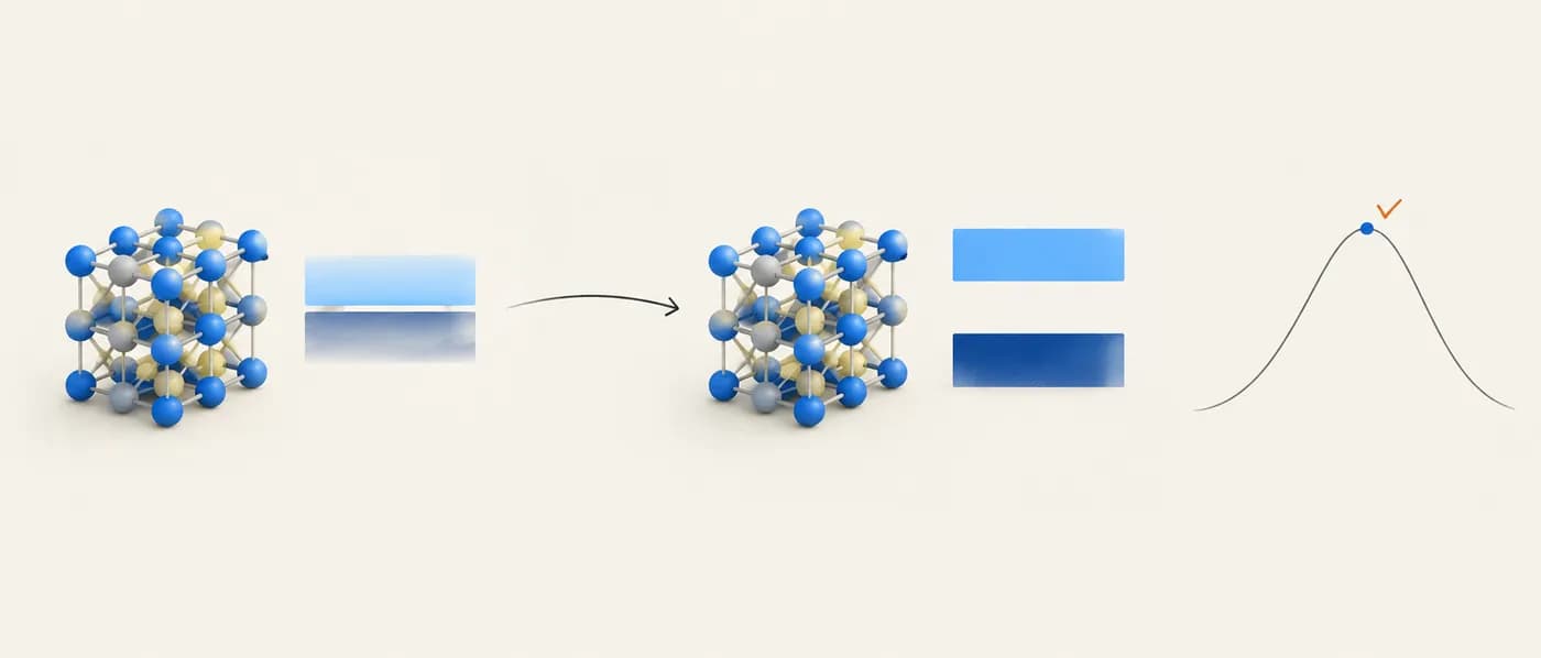
A screen returns a new chalcogenide with a PBE band gap of 0.7 eV and nearly discards it as too narrow.
- 01Recall the bias: for silicon, PBE gives ≈ 0.6 eV vs 1.12 eV measured, about half the true value.
- 02Recompute with HSE or look up a TBmBJ gap: suppose it returns 1.3 eV.
- 03Place 1.3 eV on the SQ curve: within about a point of the 33.7% maximum.
- 04Check gap type and absorption: a direct gap with strong absorption keeps it on the shortlist.
Screening on raw PBE gaps silently throws away good absorbers. Correct gaps before applying the SQ window.
Choosing a top cell for a silicon tandem
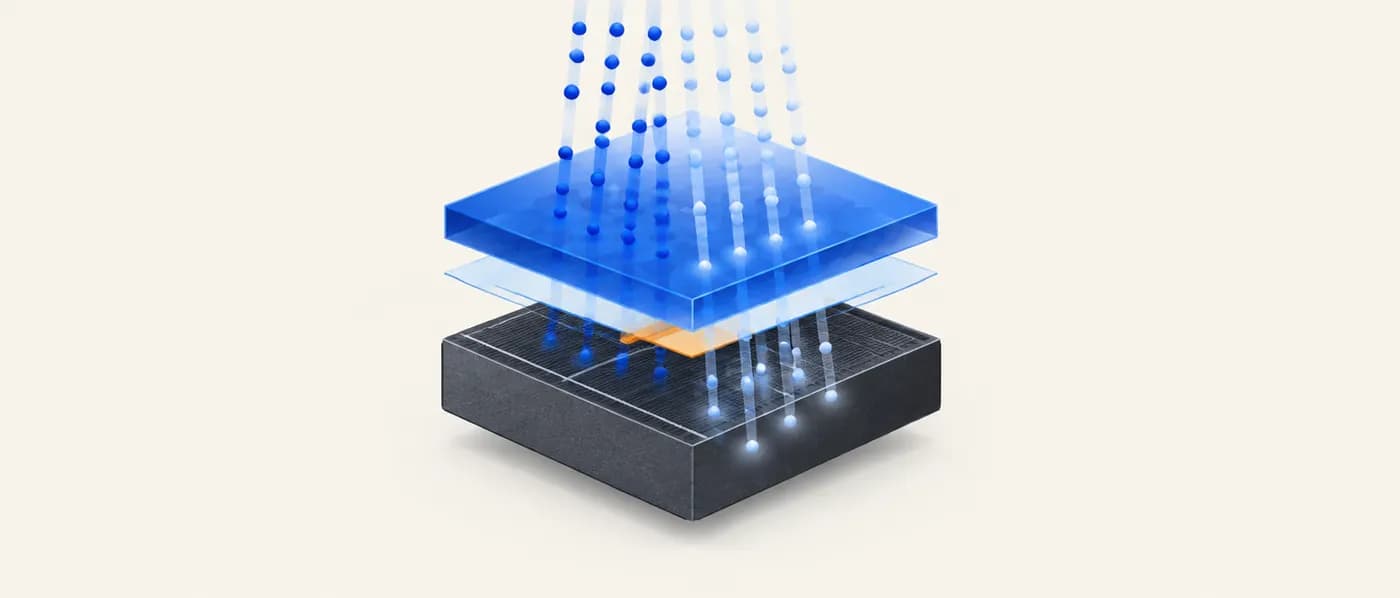
A perovskite–silicon tandem needs a top-cell gap that splits the spectrum well with silicon’s 1.12 eV.
- 01In a two-terminal tandem the currents must match, which pushes the optimal top-cell gap to roughly 1.65–1.75 eV over silicon.
- 02A 1.7 eV top cell absorbs up to ≈ 1240 / 1.7 ≈ 730 nm and passes longer wavelengths to the silicon.
- 03Mixed-halide perovskites can be tuned into this range by adjusting the iodide/bromide ratio, but halide segregation under light is a known stability risk.
- 04Compare with the single-junction SQ curve: a 1.7 eV absorber alone has a noticeably lower ceiling than at 1.34 eV, so it is a tandem play, not a stand-alone one.
A gap that is “too wide” for a single junction can be ideal in a tandem. Choose the screening window by architecture.
Band gaps of common absorbers and their place on the SQ curve (approximate)
| Absorber | Band gap (eV) | Gap type | Cut-off wavelength (nm) | Position vs SQ optimum |
|---|---|---|---|---|
| Crystalline Si | 1.12 | Indirect | ≈ 1,107 | Slightly below optimum; near the peak |
| GaAs | 1.42 | Direct | ≈ 873 | Just above optimum; near the peak |
| CdTe | ≈ 1.45–1.5 | Direct | ≈ 830–855 | Near the peak |
| CIGS (Cu(In,Ga)Se₂) | ≈ 1.0–1.2 (typical devices; tunable to ~1.7) | Direct | ≈ 1,030–1,240 | Near the peak |
| MAPbI₃ perovskite | ≈ 1.55–1.6 | Direct | ≈ 775–800 | Upper edge of the window |
| Amorphous Si | ≈ 1.7 | — | ≈ 730 | Above window; tandem-top candidate |
When to use it — and when not to
- First-pass screening of candidate absorbers by band gap.
- Explaining the efficiency ceiling of a technology to non-specialists.
- Choosing top- and bottom-cell gaps for tandem designs.
- Sanity-checking efficiency claims (a single-junction claim above ~33.7% under one sun is a red flag).
- As a prediction of real-device efficiency. Defects, interfaces and non-radiative recombination dominate in practice.
- For multi-junction, concentrator or hot-carrier concepts without the appropriate generalised limit.
- With uncorrected PBE band gaps.
Common mistakes
Applying it in Lattice Graph
LatticeGraph’s materials search lets you filter by band gap, compare gaps across sources, and see whether a value is from PBE, a higher-level method or experiment.
- 01Filter candidates to a band-gap window (for example 1.1–1.6 eV) and prefer higher-level or measured gaps where available.
- 02Open the confidence view to see how gap values from different databases agree, and flag PBE-only entries.
- 03Shortlist and export with provenance so the gap method travels with every number.
Frequently asked questions
Why is the maximum near 1.34 eV and not at silicon’s 1.12 eV?
Under AM1.5G, the balance between unabsorbed photons and thermalisation loss peaks near 1.34 eV. Silicon is slightly below the optimum but still within about a point of the maximum.
Can a solar cell beat the Shockley–Queisser limit?
A single-junction cell under one sun cannot. Multi-junction cells, concentration and certain advanced concepts can exceed it, because they change the assumptions of the calculation.
What is SLME?
Spectroscopic Limited Maximum Efficiency (Yu & Zunger, 2012) refines the SQ approach using the computed absorption spectrum and a penalty for indirect gaps, so it can rank materials with similar gaps.
Does temperature change the limit?
Yes. The standard limit assumes about 25 °C. Hotter cells have lower voltage and a lower ceiling.
References & further reading
- [1]Shockley, W. & Queisser, H. J. (1961). Detailed balance limit of efficiency of p–n junction solar cells. Journal of Applied Physics, 32(3), 510–519.Original detailed-balance limit.
- [2]Rühle, S. (2016). Tabulated values of the Shockley–Queisser limit for single junction solar cells. Solar Energy, 130, 139–147.AM1.5G tabulation; maximum ≈ 33.7% at ≈ 1.34 eV.
- [3]Yu, L. & Zunger, A. (2012). Identification of potential photovoltaic absorbers based on first-principles spectroscopic screening of materials. Physical Review Letters, 108, 068701.Introduces SLME.
- [4]Richter, A., Hermle, M. & Glunz, S. W. (2013). Reassessment of the limiting efficiency for crystalline silicon solar cells. IEEE Journal of Photovoltaics, 3(4), 1184–1191.Auger-limited silicon efficiency ≈ 29.4%.