GaO2
GaO2 is a metallic gallium-oxide compound that is structurally diverse but thermodynamically unstable compared to other common wide-bandgap oxides.
About GaO2
GaO2 is a metallic oxide compound that exists within the broader family of wide-bandgap oxide semiconductors. Despite the typical insulating nature of its class, this specific stoichiometry exhibits metallic electronic character, marking it as a unique subject for fundamental materials research. Its structural landscape is remarkably diverse, supported by a vast array of reported configurations across multiple databases. Because it resides above the thermodynamic stability hull, it is generally considered an unstable phase under standard conditions, suggesting that its synthesis requires precise control or specific stabilization techniques. This makes it a fascinating target for scientists investigating metastable oxide phases and their potential for exotic electronic properties.
Key Properties
Cross-validated computational properties for GaO2, aggregated across 4 databases.
Band GapEnergy needed to move an electron from the valence band to the conduction band. Lower or zero values tend to behave more metallic; larger gaps are more insulating or semiconducting.
Energy Above HullThermodynamic distance from the most stable set of competing phases. 0 eV/atom is on the convex hull; small positive values may still be experimentally accessible.
StabilityA plain-language summary of the best reported energy-above-hull result. It reflects whether the lowest-energy structure is on, near, or far from the stability hull.
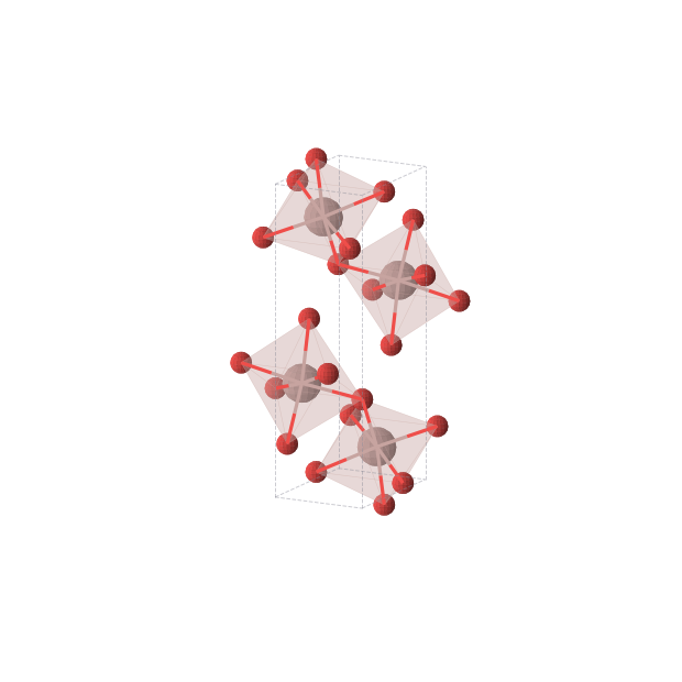
StructuresCount of reported calculated crystal structures for this formula, including alternate polymorphs, source databases, and observed space groups.
Cross-Source DFT Agreement
How well independent DFT databases agree on the thermodynamics of GaO2. Tight agreement means computed properties can be trusted without re-running calculations.
Agreement ScoreA normalized confidence score summarizing how closely independent DFT databases agree. Higher scores mean tighter cross-source agreement.
Hull SpreadDifference between the highest and lowest energy-above-hull values reported by comparable sources. Smaller spread means less thermodynamic disagreement.
Sources ComparedNumber and names of computational sources with comparable entries for this formula.
Space Group ConsensusWhether independent sources predict the same crystal symmetry for the lowest-energy structure.
Synthesis Routes
Literature-extracted synthesis procedures targeting GaO2.
Applications
Where GaO2 is used.
Frequently Asked Questions
Common questions about GaO2, answered from cross-validated data.
What is GaO2?
GaO2 is a metallic gallium-oxide compound that is structurally diverse but thermodynamically unstable compared to other common wide-bandgap oxides.
What is GaO2 used for?
What is the band gap of GaO2?
Is GaO2 a metal, semiconductor, or insulator?
Is GaO2 thermodynamically stable?
How many polymorphs of GaO2 are known?
How is GaO2 synthesized?
What elements does GaO2 contain?
Where does the data for GaO2 come from?
How It Compares
Within the wide-bandgap oxide semiconductors class.
Unlike its more stable and widely utilized siblings such as Ga2O3 or ZnO, which are prized for their robust wide-bandgap insulating properties, GaO2 stands out due to its metallic nature. While materials like Al2O3 and SnO2 are characterized by their high dielectric strength and structural reliability, GaO2 represents a more volatile member of the oxide group, offering a distinct electronic profile that deviates from the traditional semiconductor behavior seen in the rest of its class.
Related Compounds
Other Wide-Bandgap Oxide Semiconductors in the database.
Data sources & attribution
- latticegraph — Lattice Graph Materials Intelligence Platform
Analyze GaO2 in the Lattice Graph platform
Polymorph comparison, confidence scoring, supply-chain risk, and patent monitoring — across 53 integrated data sources.
Explore the Platform →