GaAs
Gallium arsenide · GaAs
Gallium arsenide is a widely used semiconductor material valued for its high electron mobility and efficiency in high-frequency electronic and optical devices.
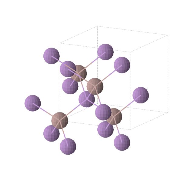
About Gallium arsenide
Gallium arsenide is a quintessential III-V semiconductor that occupies a central role in modern solid-state physics. As a thermodynamically stable compound, it serves as a foundational material for high-speed electronic devices and light-emitting technologies due to its favorable electronic properties.
Its utility stems from its ability to facilitate rapid electron transport, making it superior to traditional silicon in specific high-frequency applications. With a vast body of structural data available, it remains one of the most thoroughly characterized and reliable materials in the semiconductor industry.
Key Properties
Cross-validated computational properties for Gallium arsenide, aggregated across 4 databases.
Band GapEnergy needed to move an electron from the valence band to the conduction band. Lower or zero values tend to behave more metallic; larger gaps are more insulating or semiconducting.
Energy Above HullThermodynamic distance from the most stable set of competing phases. 0 eV/atom is on the convex hull; small positive values may still be experimentally accessible.
StabilityA plain-language summary of the best reported energy-above-hull result. It reflects whether the lowest-energy structure is on, near, or far from the stability hull.
StructuresCount of reported calculated crystal structures for this formula, including alternate polymorphs, source databases, and observed space groups.
Synthesis Routes
Literature-extracted synthesis procedures targeting GaAs.
Applications
Where Gallium arsenide is used.
Patent Landscape
18 patents reference GaAs or close compositional variants.
| Patent | Title | Assignee | Granted |
|---|---|---|---|
| 12302542 | Method of producing large EMI shielded GaAs infrared windows | — | — |
| 11017913 | Crystal and substrate of conductive GaAs, and method for forming the same | — | — |
| 5817179 | GaAs anneal boat design and method for use | — | — |
| 5834379 | Process for synthesis of cubic GaN on GaAs using NH.sub.3 in an RF plasma process | — | — |
| 5464664 | Downstream ammonia plasma passivation of GaAs | — | — |
| 5384151 | InGaAsP/GaAs diode laser | — | — |
| 5389396 | InGaAsP/GaAs diode laser | — | — |
| 11955251 | Crystal and substrate of conductive GaAs, and method for forming the same | — | — |
| 5821171 | Article comprising a gallium layer on a GaAs-based semiconductor, and method of making the article | — | — |
| 12084791 | Method of producing large EMI shielded GaAs and GaP infrared windows | — | — |
Frequently Asked Questions
Common questions about Gallium arsenide, answered from cross-validated data.
What is GaAs?
Gallium arsenide is a widely used semiconductor material valued for its high electron mobility and efficiency in high-frequency electronic and optical devices.
What is GaAs used for?
What is the band gap of GaAs?
Is GaAs a metal, semiconductor, or insulator?
Is GaAs thermodynamically stable?
How many polymorphs of GaAs are known?
How is GaAs synthesized?
What elements does GaAs contain?
Where does the data for GaAs come from?
How It Compares
Within the iii-v semiconductors class.
Within the family of III-V semiconductors, GaAs is distinguished by its balanced performance profile compared to siblings like AlAs or GaP. While materials such as GaN offer different advantages in power handling and wide-gap performance, GaAs remains the industry standard for high-frequency communication and efficient optoelectronic integration.
Related Compounds
Other III-V Semiconductors in the database.
Data sources & attribution
- latticegraph — Lattice Graph Materials Intelligence Platform
Analyze GaAs in the Lattice Graph platform
Polymorph comparison, confidence scoring, supply-chain risk, and patent monitoring — across 53 integrated data sources.
Explore the Platform →