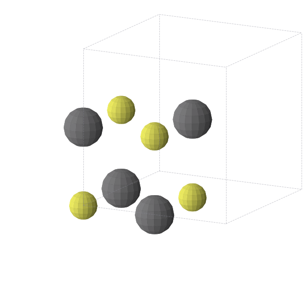
PbS
Galena · Lead sulfide
PbS is a stable, naturally occurring lead sulfide semiconductor widely used for its infrared sensing and thermoelectric capabilities.
About Galena
PbS is a thermodynamically stable lead chalcogenide that functions as a classic semiconductor. Its robust structural integrity and electronic properties make it a foundational material for studying charge transport in heavy-metal compounds.
Due to its well-documented nature and extensive structural data, this compound serves as a benchmark in materials science. It is primarily utilized in infrared detection and thermoelectric energy conversion, where its ability to manage thermal and electrical conductivity is highly valued.
Key Properties
Cross-validated computational properties for Galena, aggregated across 4 databases.
Band GapEnergy needed to move an electron from the valence band to the conduction band. Lower or zero values tend to behave more metallic; larger gaps are more insulating or semiconducting.
Energy Above HullThermodynamic distance from the most stable set of competing phases. 0 eV/atom is on the convex hull; small positive values may still be experimentally accessible.
StabilityA plain-language summary of the best reported energy-above-hull result. It reflects whether the lowest-energy structure is on, near, or far from the stability hull.
StructuresCount of reported calculated crystal structures for this formula, including alternate polymorphs, source databases, and observed space groups.
Cross-Source DFT Agreement
How well independent DFT databases agree on the thermodynamics of PbS. Tight agreement means computed properties can be trusted without re-running calculations.
Agreement ScoreA normalized confidence score summarizing how closely independent DFT databases agree. Higher scores mean tighter cross-source agreement.
Hull SpreadDifference between the highest and lowest energy-above-hull values reported by comparable sources. Smaller spread means less thermodynamic disagreement.
Sources ComparedNumber and names of computational sources with comparable entries for this formula.
Space Group ConsensusWhether independent sources predict the same crystal symmetry for the lowest-energy structure.
Synthesis Routes
Literature-extracted synthesis procedures targeting PbS.
Applications
Where Galena is used.
Patent Landscape
1 patent reference PbS or close compositional variants.
| Patent | Title | Assignee | Granted |
|---|---|---|---|
| 4029853 | PbS-Al selective solar absorber | — | — |
Frequently Asked Questions
Common questions about Galena, answered from cross-validated data.
What is PbS?
PbS is a stable, naturally occurring lead sulfide semiconductor widely used for its infrared sensing and thermoelectric capabilities.
What is PbS used for?
What is the band gap of PbS?
Is PbS a metal, semiconductor, or insulator?
Is PbS thermodynamically stable?
How many polymorphs of PbS are known?
How is PbS synthesized?
What elements does PbS contain?
Where does the data for PbS come from?
How It Compares
Within the lead chalcogenide thermoelectrics class.
Within the family of lead chalcogenides, PbS stands out as the most naturally abundant and stable member compared to its selenium-based sibling, PbSe. While other complex configurations like PbS2 or mixed-metal systems like CdPbS2 explore different stoichiometry and structural phases, PbS remains the primary reference point for the group due to its simplicity and reliable performance in semiconductor applications.
Related Compounds
Other Lead Chalcogenide Thermoelectrics in the database.
Data sources & attribution
- latticegraph — Lattice Graph Materials Intelligence Platform
Analyze PbS in the Lattice Graph platform
Polymorph comparison, confidence scoring, supply-chain risk, and patent monitoring — across 53 integrated data sources.
Explore the Platform →