Cu2SiS3
Cu2SiS3 is a semiconducting copper silicon sulfide that shows significant potential for use in emerging electronic and energy-harvesting technologies.
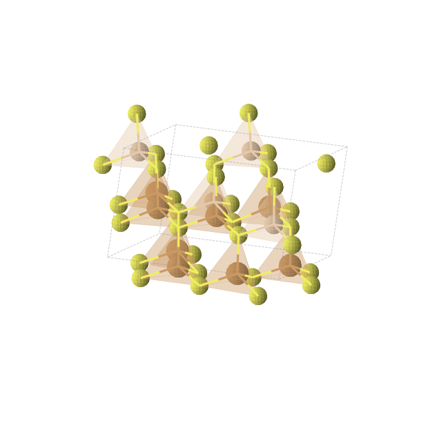
About Cu2SiS3
Cu2SiS3 is a ternary sulfide semiconductor composed of copper, silicon, and sulfur. Its electronic properties and structural versatility make it an intriguing subject for materials science research, particularly in the development of sustainable thin-film technologies.
As a near-hull stable compound, it is considered highly likely to be synthesizable in laboratory settings. The significant number of reported structures across multiple databases highlights its importance as an emerging material with potential for tunable electronic behavior.
Key Properties
Cross-validated computational properties for Cu2SiS3, aggregated across 3 databases.
Band GapEnergy needed to move an electron from the valence band to the conduction band. Lower or zero values tend to behave more metallic; larger gaps are more insulating or semiconducting.
Energy Above HullThermodynamic distance from the most stable set of competing phases. 0 eV/atom is on the convex hull; small positive values may still be experimentally accessible.
StabilityA plain-language summary of the best reported energy-above-hull result. It reflects whether the lowest-energy structure is on, near, or far from the stability hull.
StructuresCount of reported calculated crystal structures for this formula, including alternate polymorphs, source databases, and observed space groups.
Applications
Where Cu2SiS3 is used.
Frequently Asked Questions
Common questions about Cu2SiS3, answered from cross-validated data.
What is Cu2SiS3?
Cu2SiS3 is a semiconducting copper silicon sulfide that shows significant potential for use in emerging electronic and energy-harvesting technologies.
What is Cu2SiS3 used for?
What is the band gap of Cu2SiS3?
Is Cu2SiS3 a metal, semiconductor, or insulator?
Is Cu2SiS3 thermodynamically stable?
How many polymorphs of Cu2SiS3 are known?
What elements does Cu2SiS3 contain?
Where does the data for Cu2SiS3 come from?
How It Compares
As a member of the ternary sulfide family, Cu2SiS3 occupies a unique niche due to its specific elemental composition, which offers a distinct alternative to more traditional chalcogenide semiconductors. Its near-hull stability suggests it can be successfully integrated into complex material systems where precise electronic control is required.
Data sources & attribution
- latticegraph — Lattice Graph Materials Intelligence Platform
Analyze Cu2SiS3 in the Lattice Graph platform
Polymorph comparison, confidence scoring, supply-chain risk, and patent monitoring — across 53 integrated data sources.
Explore the Platform →